

SEMICON West 2026:
CCS Highlights from the Show
Thank you for joining us at SEMICON West 2026.
We hope the event provided you with valuable solutions and meaningful insights.
Here’s a brief overview of what we showcased.
For more information, please feel free to contact us.
Station 1
High-Speed Inspection for Semiconductor Wafer Surface
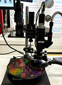
Visualize printed characters and minute defects on a high-speed rotating semiconductor wafer using the PFBR-600SW2 and a low-angle ring light guide.
The PFBR-600SW2 Series was designed by optimizing both the lighting control system and the optical system as an integrated solution, which enables higher illuminance than our conventional products, strobe operation capable of replacing xenon flash lamps, and highly linear intensity control.
Related information
- PFBR-600SW2 Series
Station 2
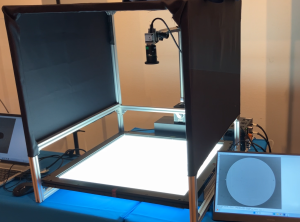
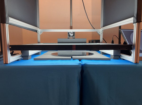
Appearance Inspection for Large Semiconductor Wafers
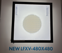
Offering a wider field of view than conventional models, the new flat dome light LFXV Series enables one-shot inspection of reflective 12-inch wafers.
Its slim design also helps minimize the overall size of the optical system.
Related information
- Flat Dome Light LFXV Series for Large Workpiece
Station 3
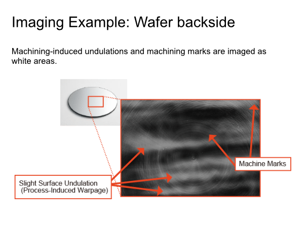
Visualization of Subtle Surface Tilt and Undulation
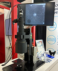
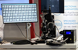
Nano- to micron-scale surface tilt and undulation on mirror-like surfaces can be visualized with high contrast using a unique polarization element.
Supports imaging with a field of view of up to approximately 110 mm.
Related information
- Polarized Pupil Division Unit
Station 4
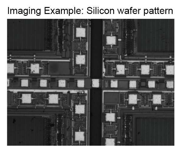
Wafer Pattern Inspection Using SWIR Lighting
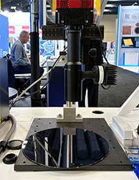
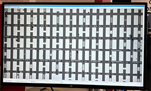
Delivering SWIR illumination that is five times brighter than our conventional imaging setup, this unit enables clear visualization of patterns through the silicon wafer surface.
Its high-output illumination supports shorter exposure times while maintaining bright, uniform images across the entire field of view.
Related information
- Lens-Integrated SWIR Lighting
Contact
For any information, please feel free to contact us.
- Web inquiry form HERE
- Email: sales@ccsamerica.com