

Visualizes nanometer-to-micrometer scale minute scratches, steps, surface irregularities, and subtle surface tilts.
Differential Interference Contrast Unit and Polarized Pupil Division Unit
Solving These Challenges
- Want to observe nano- to micron-scale scratches and surface inclination components on specular workpieces with high contrast
- Want to observe a wider area than is possible with a conventional differential interference contrast microscope
- Want to inspect minute scratches, machining marks, and warping on glossy surfaces such as mirrors and wafers
Differential Interference Contrast Unit and Polarized Pupil Division Unit
The Differential Interference Contrast Unit and Polarized Pupil Division Unit enable visualization of nanometer-to-micrometer scale minute scratches, steps, surface irregularities, and subtle surface tilts that are difficult to detect with conventional imaging methods.
Built on proprietary technology that integrates the light and lens into a unified design, the unit delivers imaging performance optimized for machine vision.
Comparison of the Differential Interference Contrast Unit and Polarized Pupil Division Unit
| Workpiece | Differential Interference Contrast Unit | Polarized Pupil Division Unit |
|---|---|---|
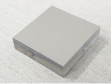 Step Height Reference Sample (40 nm) |
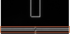 The boundary of the step is clearly visible |
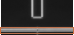 The step can be clearly observed, but the edge is blurred |
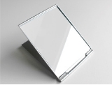 Mirror |
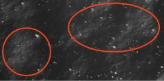 Tilt and surface undulation are only partially visible |
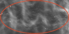 Gentle surface tilts and undulations are clearly visualized |
Differential Interference Contrast Unit
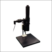
Minute surface steps can be visualized by observing interference generated by the phase difference (optical path difference) of light reflected from two closely spaced points.
Features
- Clearly visualizes minute scratches and irregularities
- Enables imaging with a wider field of view than conventional differential interference contrast microscopes
Application Example
- Inspection for minute scratches and marks on glossy surfaces
- Detection of scratches, cracks, and crystal defects on wafers
Imaging Example
Sapphire substrate*
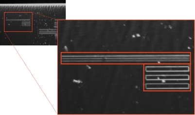
Minute height differences are clearly captured
*30 nm laser grooving
Wafer Scratches
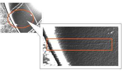
Visualize minute scratches
Polarized Pupil Division Unit
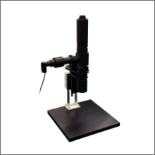
MSU-1R5RD-CMOPPD
A proprietary polarization element detects changes in polarization caused by surface inclination, enabling visualization of even subtle tilts and undulations
Features
- Visualizes subtle surface tilts and undulations using a unique polarization element
- Capable of imaging with a field of view of up to approximately 110 mm (0.1x optical magnification)
Application Example
- Inspection of fine undulations and inclinations on glossy surfaces, as well as detection of wafer polishing marks, warping, and machining marks
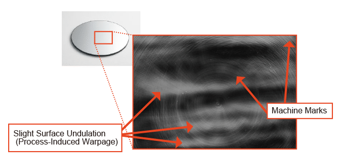
Wafer Backside
Machining-induced undulations and machining marks are imaged as white areas
Common Specifications
Please refer to the downloadable materials for specifications and dimensional drawings.
Optical Magnification Can Be Customized
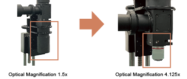
The optical magnification can be customized, including changing the sensor size to 1.1 inch and the optical magnification to 1.0x. Contact us for details.
| Available Optical Magnification Options | |||||
|---|---|---|---|---|---|
| Differential Interference Contrast Unit | 1.0x | 1.5x | 4.125x | 8.25x | 16.5x |
| Polarized Pupil Division Unit | 0.1x | 0.8x | 1.0x | 1.5x | 4.125x |